

Image-Based Particle Analysis: The Key to Precision in Semiconductor P…
페이지 정보
작성자 Erna 작성일26-01-01 00:05 조회2회 댓글0건관련링크
본문
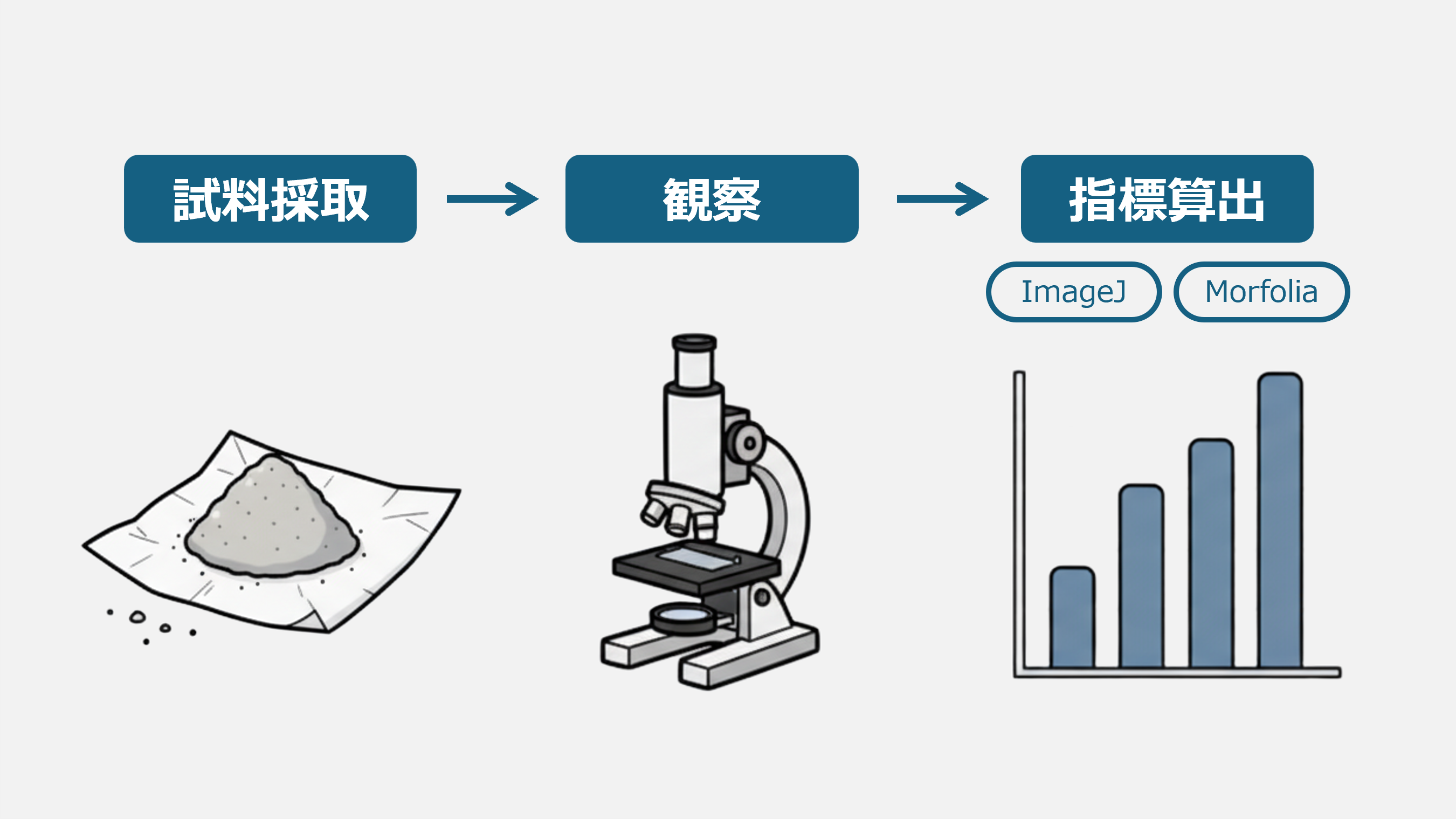
Visual contamination monitoring tools plays a vital role in chip fabrication by enabling high-resolution detection, classification, and monitoring of nanoscale particles that can compromise chip performance and production efficiency. As semiconductor features shrink to atomic-level scales, even the smallest particulate matter—often under 50nm in size—can cause electrical failures, line breaks, or non-uniform doping.
Human-driven visual checks are no longer viable due to the velocity, scale, and sensitivity required in state-of-the-art manufacturing environments. High-precision imaging solutions use high-resolution optical and electron microscopy combined with machine vision algorithms to automatically identify and characterize particles on chip surfaces, reticles, and cleanroom equipment.
These systems capture detailed images of surfaces under optimized illumination and zoom levels, then apply deep learning models and AI classifiers to filter out noise from actual defects. By analyzing parameters such as volume, geometry, count, position, and light interaction, manufacturers can identify root causes—whether from fabrication tools, HVAC units, or operator contact—and take preventive measures.
Real-time monitoring allows for instant response, 粒子径測定 reducing the likelihood of faulty chips moving into expensive processing stages.
Additionally, image-based particle analysis enables SPC systems by generating actionable analytics that can be monitored across batches. This enables manufacturers to define acceptable limits, anticipate drifts, and verify the performance of filtration and cleansing systems. Integration with factory automation systems allows for adaptive control mechanisms, where detection thresholds prompt environmental recalibrations, equipment servicing, or transport protocol changes.
This approach also meets demanding certification requirements such as SEMI F20, ISO 14644, and JESD standards, which mandate rigorous contamination control in chip manufacturing. By replacing subjective human assessment with objective, repeatable measurements, image-based particle analysis improves consistency across production sites and minimizes inter-batch differences.
Ultimately, this leads to higher yields, reduced waste, and more robust integrated circuits that meet the demands of smartphones, autonomous systems, and machine learning processors.
With ongoing advancements in scaling and chip stacking, the accuracy and throughput of image-based particle analysis will stay critically vital to maintaining quality and scalability in chip fabrication.
댓글목록
등록된 댓글이 없습니다.